8155 PPI:
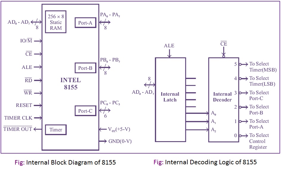
The INTEL 8155 includes 256 bytes of RAM memory, three IO ports, and a timer. The 8156 is identical to the 8155 except that the 8156 requires active high Chip Enable (CE). Functionally 8155 can be viewed as two independent chips, one having static RAM and the other having IO ports and a timer. The IO section of 8155 includes 2 numbers of 8-bit parallel IO ports called port-A and port-B, one 6-bit port called port-C, and a programmable timer.
All the ports can be configured as simple input or output ports. Ports A and B can be programmed in the handshake mode. In the handshake mode, each port uses three signals as handshake signals and the port-C pins are used for handshake signals. When some of the port-C pins are used for handshake signals, the remaining pins can be used as simple input or output lines. The timer has a 14-bit counter which can be programmed to work in four operating modes. The internal block diagram of 8155 and its internal decoding logic are shown in below Fig:

The control logic of the 8155 is specifically designed to eliminate the need for external demultiplexing of AD0 – AD7 and generate separate control signals for memory and IO. The ALE, IO/M, RD and WR signals from the 8085 can be connected directly to 8155. The ports and the timer of 8155 are IO-mapped in the system. Hence an 8-bit address is used to select the internal devices. Actually, the internal devices require a 3-bit address to select any one of the five internal devices. The remaining address lines are decoded to produce the chip select signal.