8254 Timer:
The INTEL 8254 timer has three independent counters. In each counter a count value can be loaded and the count value can be decremented by applying a clock signal. At the end of the count, each counter will generate an output that can be used as an interrupt for the processor to initiate the time-based activity. The 8254 is a 24-pin IC packed in DIP and requires a single +5-V supply. The functional block diagram of 8254 is shown in below Fig.
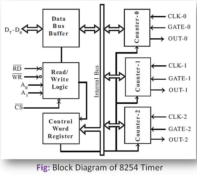
The 8254 has three independent 16-bit counters, which can be programmed to work in any one of the possible six modes. Each counter has a clock input, gate input, and counter output. To operate a counter, a count value has to be loaded in the count register, the gate should be tied high and a clock signal should be applied through clock input. The counter counts by decrementing the count value by one in each cycle of the clock signal and generates an output depending on the mode of operation. The maximum input clock frequency for 8254 is 10 MHz.
Applications of 8254 Timer:
Some of the applications of programmable timers are given below:
1. The timer can interrupt a time-sharing operating system at specified intervals so that it can switch programs.
2. The timer can send timing signals at periodic intervals to IO devices.
3. The timer can be used as a baud rate generator.
4. The timer can be used to measure the time between external events.
5. The timer can be used as an external event counter to count repetitive external operations and inform the count value of the processor.
6. The timer can be used to initiate an activity through interruption after a programmed number of external events have occurred.