Block Diagram of IC 555:
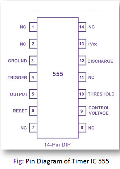
The 555 integrated circuit timer was first introduced by Signetics Corporation as Type SE555/NE555. It is available in 8-pin circular style To-99 Can, 8-pin mini DIP, and 14-pin DIP as shown below figure:
The 555 iC is widely popular and various manufacturers provide the IC. The IC 556 contains two 555 timers in a 14-pin DIP package, and Exar’s XR-2240 contains a 555 timer with a programmable binary counter in a single 16-pin package.
IC 555 Working Principle:
The IC 555 timer can be operated with a DC supply voltage ranging from +5V to +18V. This feature makes the IC compatible with TTL.CMOS logic circuits and op-amp-based circuits. The IC 555 timer is very versatile and its applications include an oscillator, pulse generator, square and ramp wave generator, one-shot multivibrator, safety alarm, timer circuits, traffic-light controllers, etc. The 555 timers can provide time delay, ranging from microseconds to hours.
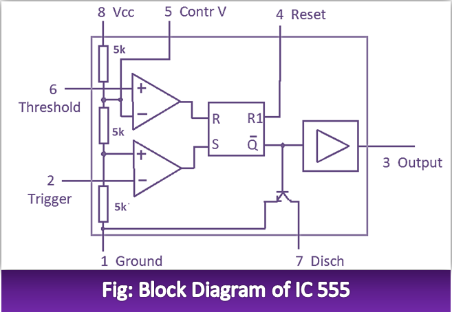
To change the output of the flip-flop to low, the voltage at the trigger input must fall below + (1/3) Vcc. When this occurs, a lower comparator triggers the flip-flop, forcing its output low. The low output from the flip-flop turns the discharge transistor off and forces the power amplifier to output a high. These conditions will continue independent of the voltage on the trigger input. The lower comparator can only cause the flip-flop to output low.