Pin Diagram of 8051 Microcontroller:
The pin configuration and the functional block diagram of 8051 are given below:
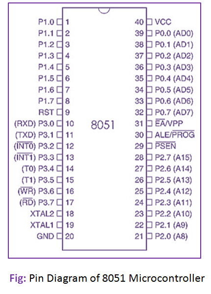
Pin 1-8: Port-1: Each of these pins can be used as either input or output according to your needs. Also, pins 1 and 2 have special functions associated with Timer 2.
Pin 9: Reset Signal: A H1 on this input halts the MCU and clears all the registers. When this pin is back to LO the program starts new as if the power had just been turned on.
Pin 10: RXD – Serial input for asynchronous communication or clock output for synchronous communication.
Pin 11: TXD – Serial output for asynchronous communication or clock output for synchronous communication.
Pin 12: INT0 – Input for interrupt 0
Pin 13: INT1 – Input for interrupt 1
Pin 14: T0 – Clock input of counter 0
Pin 15: T1 – Clock input of counter 1
Pin 16: WR – Signal for writing to external (add-on) RAM memory.
Pin 17: RD – Signal for reading from external RAM memory.
Pin 18-19: X2 – X1: Input and output of internal oscillator.
Pin 20: GND: Ground