The primary function of memory interfacing is that the microprocessor should be able to read from and write into a set of semiconductor memory IC chips. Generally, EPROM is interfaced for reading operations and RAM is interfaced for reading and writing operations. The procedure for interfacing SRAM for reading/write operation and EPROM for reading operation is similar. So, they are dealt with commonly in this section.
In order to perform the read/write operation the memory access time should be less than the read/write time of the processor, chip select signals should be generated for selecting a particular memory IC, and suitable control signals have to be generated for reading/write operation and a specific address should be allotted to each memory location.
Hence memory interfacing deals with choosing memories with suitable access time, designing an address decoding circuit to generate chip select signals, generating control signals for reading/write operation, and allocation of addresses to various memory ICs and their locations.
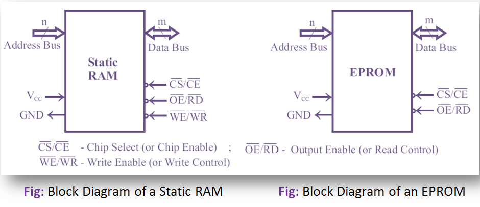
Typical EPROM and Static RAM:
A typical semiconductor memory IC will have n address pins, m data pins (or output pins), and a minimum of two power supply pins (one for connecting required supply voltage (VCC) and the other for connecting ground). The control signals needed for static RAM are chip select (chip enable), read control (output enable), and write control (write enable). The control signals needed for reading operation in EPROM are chip select (chip enable) and read control (output enable). A typical static RAM and EPROM are shown below figure respectively.
The pins of EPROM are redefined for the write operation. An EPROM requires a different hardware setup and high supply voltage for the write operation.