8085 Microprocessor Pin:
The INTEL 8085 is an 8-bit microprocessor released in the year 1976. The 8085 is designed using NMOS technology and now it is manufactured using HMOS technology and contains approximately 6500 transistors. The 8085 is packed in a 40-pin DIP (Dual In-line Package) and requires a single 5-volt supply.
The 8085 has an internal clock oscillator. It generates a clock signal internally, divides it by two, and is then used as an internal clock. This internal clock is also given out through a CLK pin for the clock requirement of peripheral devices.
The 8085 has 8 pins AD0 to AD7 for data transfer, which are multiplexed with a low byte of the address. The 8085 provides a signal ALE (Address Latch Enable) to demultiplex the low byte address and data using an external latch. The demultiplexing of address and data lines in 8085. The pin configuration diagram of the 8085 Microprocessor is given below:
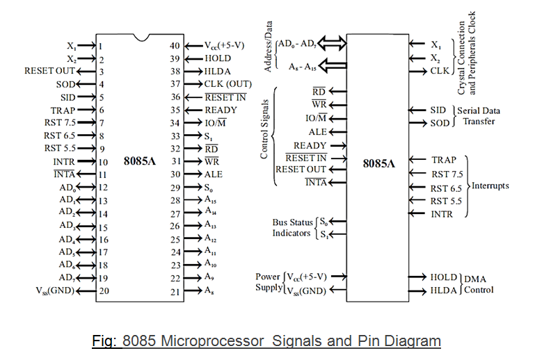
During memory access, the 16-bit memory address is output on AD0 to AD7 and A8 to A15 lines. During IO access of IO-mapped devices, the 8-bit IO address is output on both AD0 to AD7 and A8 to A15 lines. The 8085 processor differentiates the memory and IO address using the signal IO/M. When the processor output gives a memory address, the IO/M is asserted low and when the processor output provides an IO with an address, the IO/M is asserted high.
The RD signal is asserted low by the processor during a memory or IO read operation. The WR signal is asserted low by the processor during memory or IO write operation. The S0 and S1 are bus status indicators.