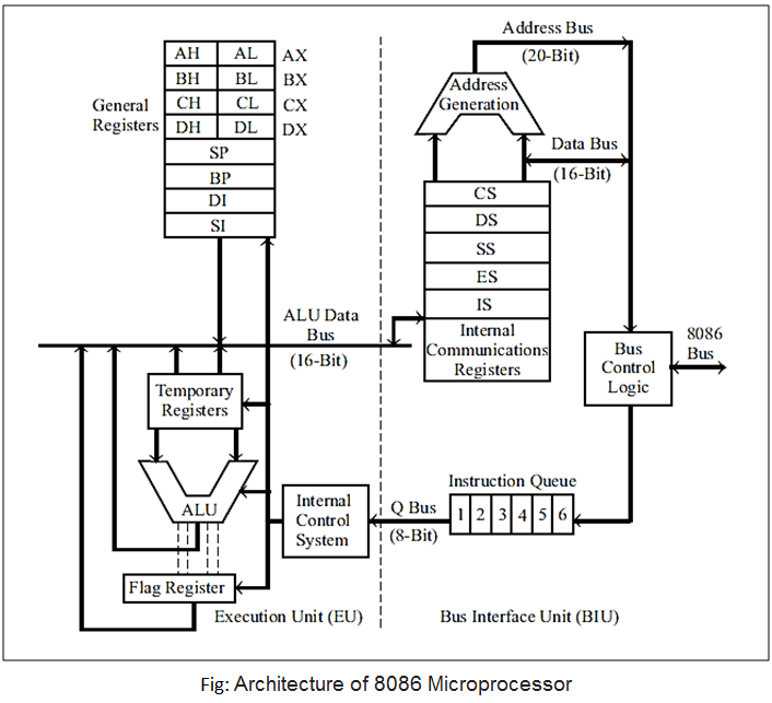
8086 Microprocessor Architecture:
8086 is the first 16-bit processor released by INTEL in the year 1978. The 8086 is designed using the HMOS technology and now it is manufactured using HMOS III technology and contains approximately 29,000 transistors. The 8086 is packed in a 40-pin DIP and requires a single 5 -volt supply.
The 8086 does not have an internal clock circuit. The 8086 requires an external asymmetric clock source with a 33% duty cycle. The 8284 clock generator is used to generate the required clock for 8086. The maximum internal clock of 8086 is 5 MHz. The other versions of 8086 with different clock rates are 8086-1, 8086-2 and 8086-4 with a maximum internal clock frequency of 10 MHz, 8 MHz and 4 MHz respectively.
The 8086 has pipelined architecture. In pipelined architecture, the processor will have several functional units and the execution time of functional units is overlapped. Each functional unit works independently most of the time. The simplified block diagram of the internal architecture of 8086 is shown below in Figure. The architecture of 8086 can be internally divided into two separate functional units: Bus Interface Unit (BIU) and Execution Unit (EU).

The BIU fetches instructions, reads data from memory and IO ports, and writes data to memory and IO ports. The BIU contains segment registers, instruction pointer, instruction queue, address generation unit and bus control unit. The EU executes instructions that have already been fetched by the BIU. The BIU and EU function independently.
The instruction queue is a FIFO (First-In-First-Out) group of registers. The size of the queue is 6 bytes. The BIU fetches instruction code from memory and stores it in the queue. The EU fetches instruction codes from the queue.
The BIU has four numbers of 16-bit segment registers. They are Code Segment (CS) register, Data Segment (DS) register, Stack Segment (SS) register and Extra Segment (ES) register. The 8086 memory space can be divided into segments of 64-kilo bytes (64kb).