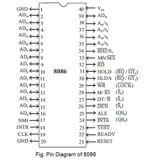
Pin Diagram of 8086:
8086 is the first 16-bit processor released by INTEL in the year 1978. The 8086 is designed using HMOS technology and now it is manufactured using HMOS III technology and contains approximately 29,000 transistors. The 8086 is packed in a 40-pin DIP and requires a single 5-volt supply.
The 8086 does not have an internal clock circuit. The 8086 requires an external asymmetric clock source with a 33% duty cycle. The 8284 clock generator is used to generate the required clock for 8086. The maximum internal clock of 8086 is 5 MHz. The other versions of 8086 with different clock rates are 8086-1, 8086-2, and 8086-4 with maximum internal clock frequencies of 10 MHz, 8 MHz, and 4 MHz respectively.
The 8086 uses a 20-bit address to access memory and hence it can directly address up to one megabyte (220 = 1Mega) of memory space. The one megabyte (1Mb) of addressable memory space of 8086 is organized as two memory banks of 512 kilobytes each (512 kb + 512 kb = 1Mb). The memory banks are called even (or lower) banks and odd (or upper) banks. The address line A0 is used to select the even bank and the control signal BHE is used to select the odd bank. For accessing IO-mapped devices, the 8086 uses a separate 16-bit address, so the 8086 can generate 64 k (216) IO addresses. The signal M/IO is used to differentiate the memory and IO addresses. For the memory address, the signal M/IO is asserted high and for IO address the signal M/IO is asserted low by the processor.
The 8086 can operate in two modes, and they are the minimum mode and the maximum mode. The mode is decided by a signal at MN/MX pin. When the MN/MX is tied high, it works in minimum mode and the system is called a uniprocessor system. When MN/MX is tied low, it works in maximum mode and the system is called a multiprocessor system. Usually, the pin MN/MX is permanently tied to low or high so that the 8086 system can work in any one of the two modes. The 8086 can work with the 8087 coprocessor in maximum mode. In this mode, an external bus controller 8288 is required to generate bus control signals.
The 8086 has two families of processors. They are 8086 and 8088. The 8088 uses an 8-bit data bus externally but the 8086 uses a 16-bit data bus externally. The 8086 can access memory in words but the 8088 can access memory in bytes. IBM designed its first Personal Computer (PC) using INTEL 8088 microprocessor as CPU. The 8086 is a 40-pin IC and all the 8086 pins are TTL compatible. The signal assigned to pins 24 to 31 will be different for the minimum and maximum modes of operation. The signal assigned to all other pins is common for minimum and maximum modes of operation.