8251 USART:
The 8251 is a programmable serial communication interface chip designed for synchronous and asynchronous serial data communication. It is packed in a 28-pin DIP. The 8251A is the enhanced version of its predecessor, 8251 and it is compatible with 8251. The functional block diagram of 8251A is shown in below Fig.
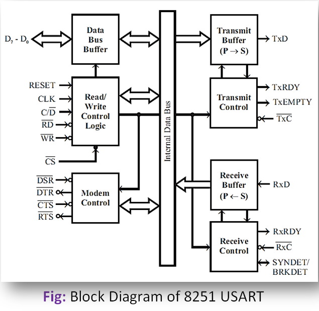
The block diagram shows five sections, they are Read/Write control logic, Transmitter, Receiver, Data bus buffer, and Modem control.
Read/Write Control Logic:
The Read/Write Control logic interfaces the 8251A with the CPU, determines the functions of the 8251A according to the control word written into its control register, and monitors the data flow. This section has three registers and they are the control register, the status register, and the data buffer.
The signals RD, WR, C/D, and CS are used for read/write operations with these registers. When C/D is high, the control register is selected for writing the control words or reading the status words. When C/D is low, the data buffer is selected for read/write operation.
Transmitter Section:
The transmitter section accepts parallel data from the CPU and converts them into serial data. The transmitter section is double buffered, i.e., it has a buffer register to hold 8-bit parallel data and another register called an output register to convert the previous data into a stream of serial bits.
The processor loads data into the buffer register. When the output register is empty, the data is transferred from the buffer to the output register. Now the processor can again load another data in the buffer register. If the buffer register is empty, then TxRDY is asserted high and if the output register is empty then TxEMPTY is asserted high. These signals can also be used as interrupts or statuses for data transmission.
Receiver Section:
The receiver section accepts serial data and converts them into parallel data. The receiver section is double buffered, i.e., it has an input register to receive serial data and convert it to parallel and a buffer register to hold the previously converted data.
Normally RxD line is high, when the RxD line goes low, the control logic assumes it is a START bit waits for half a bit of time, and samples the line again. If the line is still low, then the input register accepts the following bits, forms a character, and loads it into the buffer register. The CPU reads the parallel data from the buffer register.
MODEM Control:
The MODEM control unit allows to interface of a MODEM to 8251A and to establish data communication through MODEM over telephone lines. This unit takes care of handshake signals for the MODEM interface.