Semiconductor Memory:
The main or primary memory elements are semiconductor devices because the semiconductor devices alone can work at high speeds and consume less power. Moreover, they can be fabricated as ICs and also occupy less space. A typical semiconductor memory IC will have n address pins (lines) and m data pins (lines). The capacity of the memory will be 2n × m bits.
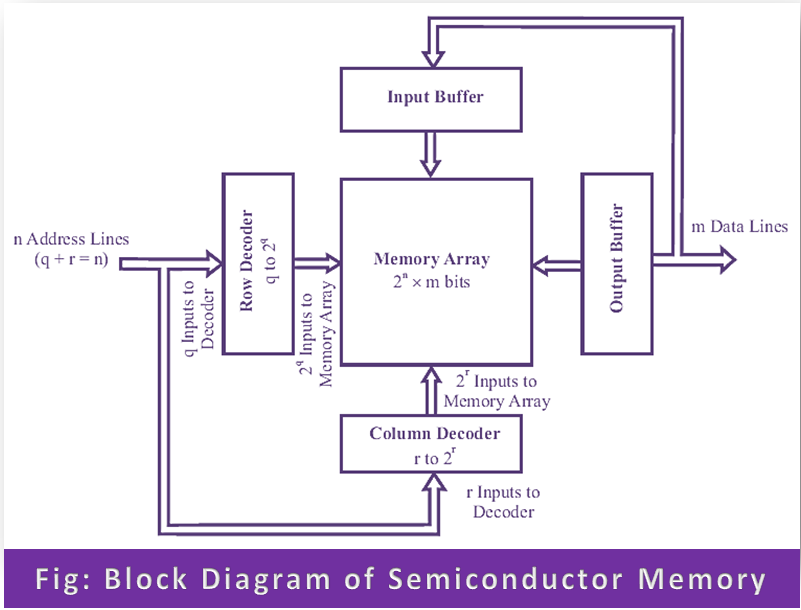
The above figure shows a simplified functional block diagram of semiconductor memory. The functional blocks of semiconductor memory are the row address decoder, column address decoder, memory array, input buffer, and output buffer.
Input and output buffers are used to hold the data until a valid time and also take care of signal current level matching (or Impedance matching). The n address lines are split into ‘q’ lines and ‘r’ lines, such that q + r = n. The ‘q’ address lines are applied as input to the row decoder and the ‘r’ address lines are applied as input to the column decoder.