Cypress CMOS:
The Cypress CMOS is a high-performance 8192 byte (8 kb) CMOS EPROM. It has power down mode, in which the device will enter a low-power standby mode when it is not enabled (or deselected). The logic block diagram of Cypress CMOS is shown below figure. The chip has thirteen address inputs denoted as A0 – A12.
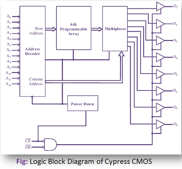
The address is used to access any one of the 8 kilos (8192) locations within the chip. The eight output lines, O0 to O7 are used to output data from the chip. The chip will be in standby mode when CE is inactive. The CE is activated for selecting the chip and OE is activated for enabling the output buffer during the reading operation.