8237 DMA Controller:
The DMA controller-8237 has been developed for the 8085/8086/8088 microprocessor-based systems. It is a device dedicated to performing a high-speed data transfer between the memory and the IO device. The 8237 has four channels. So, it can be used to provide DMA to four IO devices. When more than four devices require DMA, a number of 8237 can be connected in cascade to increase the DMA channels.
For each DMA channel, a set of registers has been dedicated to storing the memory address and the count value for a number of bytes to be read/written by DMA. These registers are base address, current address, base word count, current word count, and mode registers. Apart from these dedicated registers, the 8237 has temporary registers, status, command, mask and request registers.
Pin Diagram of 8237 DMA Controller:
The 8237 is a 40-pin IC and is available in a Dual In-line Package (DIP). The pin configuration diagram of 8237 is shown in below Fig.
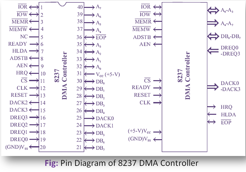
CLK: Clock input to 8237. The maximum clock frequency is 5 MHz. In the 8085 system, the processor clock is inverted and applied to CLK 8237.
CS: Logic low chip select signal. It is an input signal to select 8237 during programming mode.
RESET: Reset input to 8237. Connected to a system reset, when the RESET signal goes high the command, status, request, and temporary registers are cleared. It also clears the first-last flip-flop and sets the mask register.
READY: Ready input signal and it is tied to VCC for normal timings. When READY input is tied low, the 8237 enters a wait state. This is used to get extra time in DMA machine cycles to transfer data between slow memory and IO devices.
HRQ: Hold request output signal. It is the hold request signal sent by 8237 to the processor HOLD pin, to make a request for the bus to perform a DMA transfer.
HLDA: Hold acknowledge input signal. It is the hold acknowledge signal to be sent by the processor to inform the acceptance of the hold request.
DREQ3 – DREQ0: DMA request inputs (Four channel inputs). Used by IO devices to request for DMA to transfer.
DACK3 – DACK0: DMA acknowledge output signals. These are output signals from 8237 to the IO devices to inform the acceptance of the DMA request. These outputs are programmable as either.
DB7 – DB0: Data bus lines. These pins are used for data transfer between the processor and DMA.
IOR: Bidirectional IO read control signal. It is an input control signal for reading the DMA controller during programming mode and an output control signal for reading the IO device during DMA (memory) write cycle.
IOW: Bidirectional IO writes control signal. It is an input control signal for writing the DMA controller during programming mode and an output control signal for writing the IO device during DMA (memory) read cycle.
EOP: End of process. It is a bidirectional low active signal. It is used either as an input to terminate a DMA process or as an output to inform the end of the DMA transfer to the processor. This output can be used as an interrupt to terminate DMA.
A3 – A0: Four bidirectional address lines. Used as input address during programming mode to select internal registers. During DMA mode the low-order four bits of memory address are output by 8237 on these lines.
A7 – A4: Four unidirectional address lines. Used to output the memory address bits A7 to A4 during DMA mode.
AEN: Address enable output signal. It is used to enable the address latch connected to DB7 – DB0 pins of 8237. It is also used to disable any buffers in the system connected to the processor.
ADSTB: Address strobe output signal. It is used to latch the high-byte memory address issued through DB7 to DB0 lines by 8237 during DMA mode into an external latch.
MEMR: Memory read control signal. It is an output control signal issued during a DMA read operation.
MEMW: Memory write control signal. It is an output control signal issued during DMA write operation.